Search This Supplers Products:BMS Boardaluminium pcbflex PCB boardsmultilayer PCBPCB AssemblyPCB Reverse Engineering
What does layer mean for pcb?
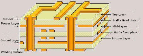
Signal Layers
Signal Layer includes Top Layer, Bottom Layer, Mid Layer 1... 30. Mid layer refers to the intermediate plate layer used for wiring, in which the conductor is arranged.
Top Layer is also called the component Layer, which is mainly used for placing components. For the double sided pcb and multilayer pcb, it can be used to arrange wires or cover copper.
Bottom Layer, also known as the welding layer, is mainly used for wiring and welding. For the double sided and multilayer pcb, it can be used to place components.
Mid-Layers can be up to 30 Layers, and are used to lay signal lines in multilayer pcb, excluding power and ground lines.
Internal Plane
This type of layer is only used for multi-layer pcb. These layers are generally connected to ground and power supply, and also have electrical connection. However, this layer is generally not wired and is composed of the whole copper film.
The number of PCB plates generally refers to the sum of the signal layer and the Internal Plane.
Silkscreen Overlay
A PCB board can have up to 2 silk-screen layers. Includes Top overlay and Bottom overlay. It is usually printed on the resistance welding layer, such as component name, component symbol, component pin and copyright, etc., to facilitate future circuit welding and error checking.If all marks in the Top overlay are already included, the Bottom overlay can be closed.
Solder Mask
Refers to the part of the PCB board to be covered with green oil; Because it is negative output, the actual effect of the soldermask part is not green oil, but tinned !
Resistance welding layer means to open a window on the whole resistance welding green oil, in order to allow welding;
By default, green oil is applied to all areas without a resistance layer