
Search This Supplers Products:BMS Boardaluminium pcbflex PCB boardsmultilayer PCBPCB AssemblyPCB Reverse Engineering
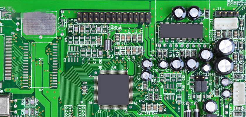
Common problems with pcb SMT for print circuit board manufacturing
EMPTY WELDING:
When two solders are heated differently or one of them has oxidation layer and dirt on the surface, the molten tin will adhere to the solder pad of the solder with higher temperature and clean surface, but not to the solder with low temperature and dirty surface, so that there is still a way between the two solders.
THE FALSE WELDING:
One of the two soldered bodies has an oxide layer or impurity on its surface, and the molten tin completely covers the soldered body. The two soldered bodies appear to be well connected, but due to the separation of oxide layer and dirt, the conductivity between the two soldered bodies is extremely poor.
VIRTUAL WELDING:
When two soldered bodies are heated unevenly or the surface of one of them is not very clean, the molten tin is less adhered to the solder plate with a lower temperature and not very clean; Or the welding technique is not correct, so that the molten tin is not evenly and fully attached to the two soldered bodies on the welding plate, the two soldered bodies although the conduction but poor electrical conductivity.
COLD WELDING:
In the welding process, due to the low welding temperature and short welding time, the tin is not enough time to fully melt, rosin is not volatilized clean and then remove the ferrochrome, so that the connection between the two soldered bodies is not strong and the electrical conductivity is not good, the position of the mouth is dirty, there is a lot of dirt.
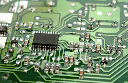
Causes of defective hollow welding and false welding in pcb manufacturing process:
A. device pin oxidation or other impurities leading to poor
B. Substrate pad design leading to poor
C. Small openings in the PCB stencil and less tin in the weld lead to poor
D. Deformation of device pins leads to poor
E. Poor quality of solder paste and poor solderability lead to poor
F. inappropriate production of temperature curve setting, resulting in poor
G. defect of reflux furnace itself, too large T lead to bad
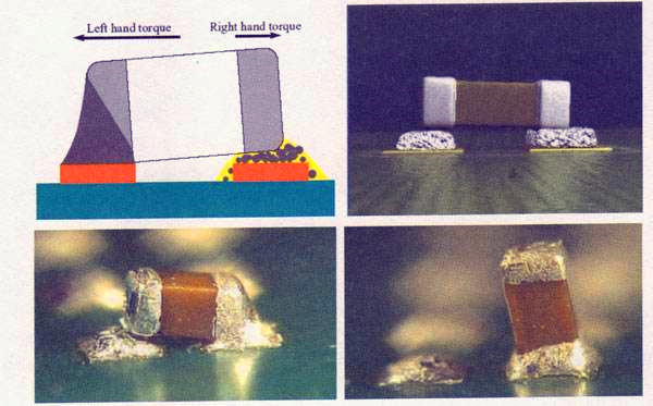
Reasons for short circuit caused by poor printing in pcb manufacturing process:
A. Insufficient metal content of solder paste, resulting in collapse
B. excessive opening of PCB stencil, resulting in excessive tin content
C. PCB stencil quality is not good, tin is not good, change laser cutting template
D. PCB stencil has solder paste on its back to reduce scraper pressure and adopt appropriate VACCUM and SOLVENT
PCB Assembly profile for the main purpose of the project
A. Preheating zone: solvent volatilization in solder paste
B. Homogenizing zone: flux activation, removal of oxides; evaporation of excess water
C. Re-soldering zone: solder melting
D. Cooling zone: alloy solder joint formation, parts foot and pad joints as a whole
In SMT process, the main causes of tin beads are as follows:
A.PCB_PAD design is not good
B.PCB stencil opening design is not good
C.Placement depth or pressure is too high
D.Profile curve rise slope is too large
E.Paste collapse, paste viscosity is too low