
Search This Supplers Products:BMS Boardaluminium pcbflex PCB boardsmultilayer PCBPCB AssemblyPCB Reverse Engineering
What is the differrence between PCB and PCBA?
PCB stands for Printed circuit board, which is the chips that supports and electrically connects electronic components or electrical components using conductive tracks, pads and other features etched from one or more sheet layers of copper laminated onto and/or between sheet layers of a non-conductive substrate.
PCBA stands for PCB assembly, which is the process of assemble all the electronic component and devices on the bare PCB. Normally it will comes with a bill of materials, which refers to the cost of devices that is being used for the PCB,e.g., resistors, diodes, transistors, etc.
There are primarily two types of assembly methods:
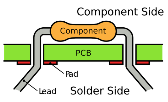
THD (Thru-Hole Device)
Thru-hole technology is accomplished by collaborating manual and automation procedure. It involves three steps as well – components placement, inspection and rectification, and wave soldering. Components placement is manually done by the technician of electronics manufacturer. Components are quickly and precisely placed in their corresponding positions. Inspection and rectification involves checking out if the components are accurately placed and rectified if an error exists. Wave soldering is the process by which the board is passed through a wave of liquid solder with a temperature of 500° Fahrenheit.
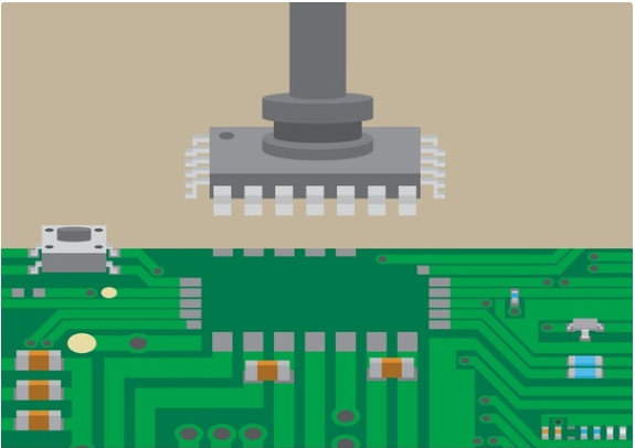
SMT (Surface-Mount Technology)
Surface mount technology is best suited to small sized components and integrated circuits. Surface mount technology features a totally automatic mounting PCB Assembly process. Surface Mount Technology follows three steps in general. The first step is the solder paste printing wherein a solder paste is applied on the board through a solder paste printer. It is very important that the solder paste used is of quality and is applied properly in order to avoid applying it again. The second step is components mounting through components reel in the machine. The last step is the reflow soldering where the board is passed through a 23-foot, 500° Fahrenheit furnace to liquefy the solder paste in order for the SMD components to firmly stick to the board.
The steps of PCB assembly process :
Solder Paste Stenciling
Pick and Place
Reflow Soldering
Inspection and Quality Control:
Manual checks
Automatic optical inspection
X-ray inspection
Through-Hole Component Insertion
Manual soldering
Wave soldering
Final Inspection and Functional Test
PCB manufacturing, the process of PCB fabrication, e.g.,making the bare board, and PCB assembly are the the two steps of finishing a “functionable” PCB. It is the key step in the turnkey electronic manufacturing services.
Most of the PCB is made out in China. China PCB manufacturer tends to congregate in a city called Shenzhen, which is now considered as silicon valley of hardware and it has a significant advantages in labor cost when it comes to PCB assembly compared to PCB manufacturers in USA.