Search This Supplers Products:BMS Boardaluminium pcbflex PCB boardsmultilayer PCBPCB AssemblyPCB Reverse Engineering
PCB Manufacturing Process
time2017/10/24

- PCB Manufacturing Process with quick turn service
PCB Manufacturing Process has passed 100% quality test

Do you know how to design and manufacturing pcbs?
There are a lot of tutorials and articles online about how to design PCBs. However, as a designer, you may be curious that how to make your board.
As a pcb circuit board factory for more than 8 years and we have lots of experience to help designers from ideas to prototype, to even mass production. Kingfung PCB Factory is a one stop prototype service which can help you prototype pcb at low cost .
Here we will introduce you the whole pcb manufacturing process in our pcb factory. There are 20 steps for the PCB manufacturing. Here is the brief introduction of the process.Wish it can help you understand pcb manufacture process.
1. Cut the raw material to a suitable size
Many printed circuit board customers usually use FR4 130-140 as the manufacturing material for prototype. The raw material original size is 41*45 inch. We will use the cutting machine to cut to board into 40*50 cm, which is suitable for manufacturing.
2. Drill hole
The min hole size is from 0.2mm to 0.3mm. Usually, the average requirement for drill hole is 0.3mm. The factory need to own strict equipment if the pcb requires smaller hole size
3. Electroless plating copper
After drilling hole, there is no copper inside the hole, meaning the holes are not contacted. So we need to make sure the holes are contacted.After electroless plating copper, there will be copper inside the holes and they are contacted.
4. Pressed film
In this step there will be a blue dry film on the board.Drying the film is a very important carrier in PCB fabrication process.
5. Exposure
Matching the route film and the board with blue dried film in the exposure machine. Under the lighting of the exposure machine, the film without route will be totally exposed. After this step, the circuit will be transferred to the dry film.
6. Develop
For the parts that are not exposed in last step, we will use the develop liquid in developer to develop.
7. cathode copper(Electric copper )
Put the board in the electric copper machine. The boards with copper will be electric and the dry film have no influenced
8. Electric tin
Electric tin is to take away the copper which is protected by the dry film.
9. Film removal
This step is to take away the blue dry film.
10. Etching
We use liquid to etch the useless copper in the board.
11. Tin removal
We use liquid to take away the tin in the board.
12. AOI route scan
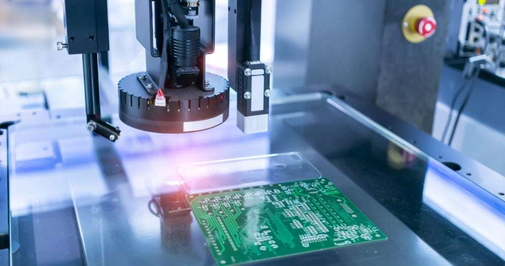
During the pcb manufacture process,because there are different issues, some pcb board will be unqualified. In order to make sure the quality of the board, we used Automatic Optical Detector (AOI) to test the circuit.
13. Print solder mask
Normally the solder mask color is green. But you also can chose other color,such as blue,black,red,and white according to your needs and requirement.
14. Solder mask exposure and develop
Putting the solder resist film on the board and exposing in the exposure machine
15. Character
We print the logo and company and other character in the board in this step.Of course,you also can chose color that you need.
16. Surface finish
It means different surface finish in this step. We can provide 7 types of surface finish for you,such as ENIG,Flash Gold, HAL-LF, HAL, Chem.Tin,Chem.Ag,OSP.
17. Rim
You can send your gerber file o describe the shape of your board. In this step, according to your Gerber file,we will use rim your board .
18. Flying Probe Test
This test is very significant during pcb manufacturing process because it is the last step of PCB fabrication with machine and it will test pcb board quality and make sure those unqualified boards will not be passed to the next step.
19. FQC
We still need to have strictly inspection for the quantity, shape and silk screen.
20. Package and Ship
After we finish the 19 steps, we will pack your boards and
Maybe it’s helpful to you:
Web link
