Search This Supplers Products:BMS Boardaluminium pcbflex PCB boardsmultilayer PCBPCB AssemblyPCB Reverse Engineering
The composition and appearance of PBC
time2017/11/04
- The composition and appearance of circuit board is the function of service.Play a huge role in composition and appearance of the PBC for its function.
The composition and appearance of PBC
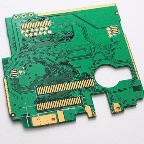
A PBC is mainly composed of the following components, line and surface (pattern): as the original line between the turn-on of the tool will also design the large copper surfaces as the ground and power planes in the design. At the same time line and the surface is made. The dielectric layer (dielectric): used to keep the insulation between the lines and each layer, commonly known as the substrate. The hole (through hole / via): via the two levels above the line mutual conduction, large holes is used in parts, non conducting hole (npth) is usually used as a surface mount assembly positioning. When the fixed screw. Soldermasks (solder resistant /solder mask): copper surface is not all to eat tin parts, so the non tin area, will be printed with a layer of insulation material copper tin (usually epoxy resin), avoid non tin line according to the different short circuit. Process points For the green, blue screen. Chili oil, oil (legend /marking/silk screen): This is not necessary, the main function is to mark the name of each component on the circuit board position frame, convenient assembly and maintenance. The composition and appearance of circuit board is the function of servic
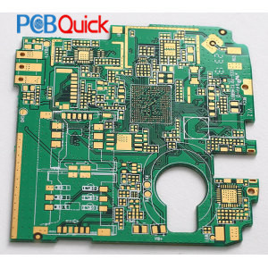
After identification by surface treatment (surface finish): the copper surface in the general environment, it is easy to oxidation of lead to tin (poor solderability), thus protect the copper surface to eat in the tin. The spray tin (HASL), gold (ENIG), silver (immersion silver), tin (immersion tin), method, the there are advantages and disadvantages, collectively referred to as surface treatment. The appearance of bare board (there are no parts) are often referred to as "printed wiring board printed circuit board (PWB). The substrate of the board itself is an insulating material, the bending is not easy. In fine lines can be seen on the surface of the material is copper, originally the copper foil is covered In the board, and in the manufacturing process partly etched off, left to the part of a network of thin wires. These lines are called conductors (conductor pattern) or wiring, and used to provide PCB parts of the circuit connection. Usually the PCB color is green or brown, this is resistance welding (solder mask). The color is a protective layer of insulation, can also prevent the short-circuit protection of copper wire, wave soldering cause, and save the amount of solder. A layer of screen printing surface in the solder layer will be printed on the (silk screen). Usually on this surface (words and symbols printed on mostly white), to indicate the position of each part in the board. Also called icon screen printing surface (legend). In the finished products, it will install integrated circuits, transistors, diodes and passive components (such as resistance, capacitance, and other connectors) A variety of electronic components. Through wire connectivity, can form the electronic signal link and should be functional. The composition and appearance of the PBC play a unique role for its function.
Play a huge role in composition and appearance of the PBC for its function. The composition and appearance of circuit board is the function of service.The composition and appearance of the PBC play a unique role for its function.
Maybe it’s helpful to you:
Web link