
Search This Supplers Products:BMS Boardaluminium pcbflex PCB boardsmultilayer PCBPCB AssemblyPCB Reverse Engineering
Copy board reverse principle
publisherJason
time2021/07/28

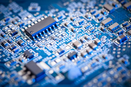
- The reverse principle of PCB is to explain the principle and working condition of the circuit board according to the reverse principle diagram, so as to analyze the functional characteristics of the product itself.
The reverse principle of PCB is to explain the principle and working condition of the circuit board according to the reverse principle diagram, so as to analyze the functional characteristics of the product itself. The principle diagram refers to the circuit diagram of PCB based on the PCB file diagram or the circuit diagram of PCB based on the actual product. In the forward design, the development of general products should first carry out schematic design, and then PCB design according to schematic design.
PCB schematic diagram plays a special role, whether it is used to analyze the circuit board principle and product performance in reverse study or reapplied to PCB design basis and basis in forward design. Then, according to the file diagram or the physical object, how to carry out the backtrace of PCB schematic diagram, the backtrace process should pay attention to those details?
1. Reasonable division of functional areas
In the reverse design of a sound PCB circuit board, reasonable division of functional areas can help engineers reduce unnecessary trouble and improve the efficiency of drawing. In general, components with the same function on a PCB board will be arranged in a centralized way, and the area divided by the function can be conveniently and accurately based on the reverse schematic diagram.
However, this division of functional areas is not arbitrary. It requires engineers to have some knowledge of electronic circuits. First, find out the core elements of a functional unit, and then find out other elements of the same functional unit by following the routing connection, forming a functional division. The formation of functional zoning is the basis of schematic drawing. Also, in the process, don't forget to use the component Numbers on the circuit board in a clever way, they can help you to quickly partition the functionality.
2. Correctly distinguish lines and reasonably draw wiring
For the distinction of ground wire, power cord and signal wire, the engineer should also have relevant power supply knowledge, circuit connection knowledge, PCB wiring knowledge and so on. The division of these circuits can be analyzed from the connection of components, width of copper foil and characteristics of electronic products.
In wiring drawing, in order to avoid line crossing and interpenetration, grounding symbols can be used for a large number of ground lines, different lines can be used for different colors to ensure clarity and discrimination, special marks can be used for various components, and even unit circuits can be drawn separately and then combined.
3. Find the right benchmark
This reference piece can also be said to be the main part adopted at the beginning of schematic drawing. After determining the reference piece, drawing according to the pins of these reference pieces can guarantee the accuracy of schematic diagram to a greater extent.
Benchmark for engineers, a sure is not very complicated things, in general, can choose to play a leading role in the circuit components as a benchmark, they generally larger, pin more, convenient drawing, such as integrated circuit, transformer, transistor, etc., are suitable as a benchmark.
4. Master the basic framework and refer to the similar schematic diagram
For the frame composition and principle drawing method of some basic electronic circuits, engineers need to be proficient, not only to be able to directly draw the basic form of some simple and classic unit circuits, but also to form the overall framework of electronic circuits.
On the other hand, it should not be neglected that the same type of electronic products have certain similarities in the schematic diagram. Engineers can draw on the same kind of schematic diagram to carry out the reverse calculation of the schematic diagram of new products based on the accumulation of experience.
V. check and optimize
After the schematic drawing is completed, the reverse design of PCB schematic diagram will be completed after testing and checking. The nominal values of components sensitive to PCB distribution parameters need to be checked and optimized. According to the PCB file diagram, the schematic diagram is compared and analyzed and checked to ensure that the schematic diagram is completely consistent with the file diagram.
Above is the detailed introduction of the reverse principle of PCB copying board, hoping to help you, you can call the consulting hotline for more information.

Maybe it’s helpful to you:


