Search This Supplers Products:BMS Boardaluminium pcbflex PCB boardsmultilayer PCBPCB AssemblyPCB Reverse Engineering
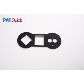
Single layer pcb manufacturing process:Double Sided Soldermask With Plating Copper Word


- group name
- Single Sided PCB Manufacturing
- Min Order
- 1 piece
- brand name
- PCBQuick PCB Manufacturing and Assembly
- model
- KF-01
- Nearest port for product export
- SZ
- Delivery clauses under the trade mode
- FOB, EXW, DDU, Express Delivery
- Acceptable payment methods
- T/T, PayPal, Westem Union, Cash, Escrow
- Export mode
- Export through agents
- update time
- Fri, 29 Oct 2021 11:14:01 GMT
Paramtents
Material FR4
Board Thickness 1.6mm
Copper Thickness 35um
Soldermask Color Black
Silkscreen Color White
Surface Technics ENIG
Min Holes 0.2mm
Min Line Width and space 5mil/5mil
Packging & Delivery
-
Min Order1 piece
Briefing
Printed Wiring Board:Single sided pcb,Plating Copper Word made with FR4 base have rigid laminate of woven glass epoxy material
Detailed
Single layer pcb manufacturing process:
On a typical PCB, the characters we see are usually painted in plain paint. However, some special circuit boards use copper as raw material for character marking.
A function of printing characters in copper is simply to look good. Use as nonferrous metal in product labeling can indirectly improve product image and brand value.
Another function of copper screen printing is to open the window in the stratum. As the foundation of electronic products, it links each component and keeps the current unobstructed. However, it is inevitable to generate heating in the working engineering. If the excessive heat cannot be spread out, it will not only hinder the current seriously, but also burn the circuit and cause damage. So the designers came up with an ingenious way of making the copper layer directly exposed to the air, which would allow it to dissipate heat more efficiently. So the designers combined the silk-layer characters on the surface of the printing plate to create a new process that combines thermal and expressive features - ground windowing.This technique is particularly common in high-power electronics。
Maybe it’s helpful to you:
Web link:


