Search This Supplers Products:BMS Boardaluminium pcbflex PCB boardsmultilayer PCBPCB AssemblyPCB Reverse Engineering
high density interconnect pcb 6Layer Blind Buried Via HDI PCB


- group name
- Special PCB Manufacturing
- Min Order
- 1 piece
- brand name
- PCBQuick PCB Manufacturing and Assembly
- model
- KF-HDI PCB-03
- Nearest port for product export
- SZ
- Delivery clauses under the trade mode
- FOB, EXW, DDU, Express Delivery
- Acceptable payment methods
- T/T, PayPal, Westem Union, Cash, Escrow
- Export mode
- Export through agents
- update time
- Fri, 19 Apr 2024 09:56:10 GMT
Paramtents
Material FR4
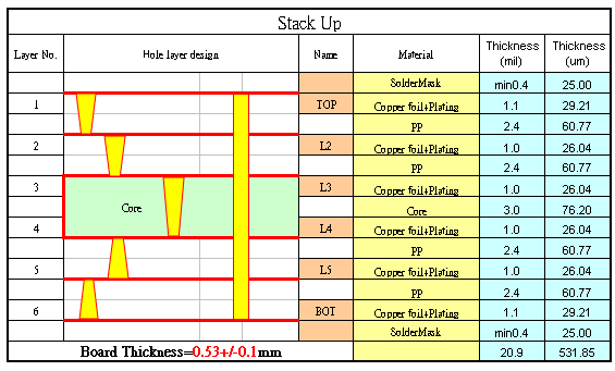
Board Thickness 0.53+/-0.1mm
Copper Thickness Inner layer 17um,External layer
Soldermask Color Green
Silkscreen Color White
Surface Technics ENIG
Packging & Delivery
-
Min Order1 piece
Briefing
HDI with quick turn service
HDI PCB with high-quality at factory price
HDI PCB with high-quality at factory price
Detailed
high density interconnect pcb 6Layer Blind Buried Via HDI PCB
Product Description
Board Thickness: 0.53+/-0.1mm
Soldermask Color: Green
Surface Technics: ENIG(Au min 1.2uinch,Ni min 100uinch)
Min Line width and space:3mil/3mil
<p vertical-align:baseline;line-height:1.2;color:#555555;white-space:normal;background-color:#ffffff;"="" style="word-wrap: break-word; margin: 0px; font-family: "sans serif", tahoma, verdana, helvetica; box-sizing: border-box; padding: 0px; border-width: 0px; border-style: initial; border-color: initial; font-size: 14px;">BGA 0.5mmDrill layer stack up: L1-L2,L2-L3,L3-L4,L4-L5,L5-L6,L1-L6
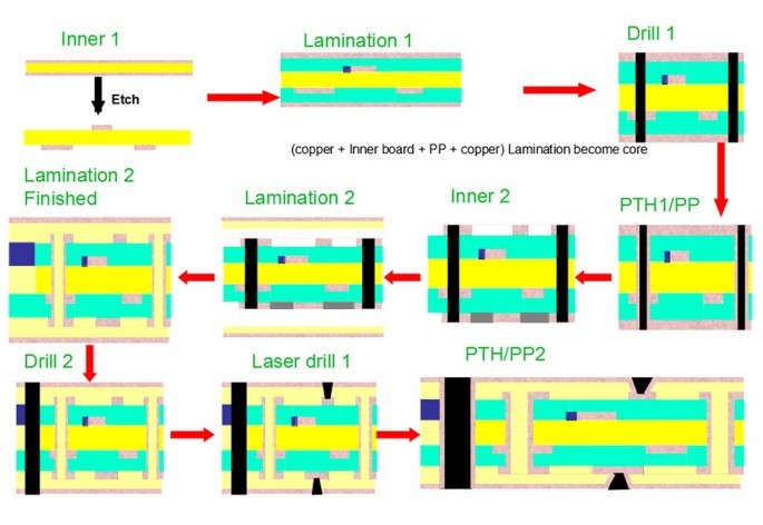
HDI PCB Manufacturing Process
HDI PCB Stack Up