Search This Supplers Products:BMS Boardaluminium pcbflex PCB boardsmultilayer PCBPCB AssemblyPCB Reverse Engineering
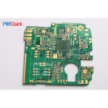
High TG Multilayer PCB printed circuit board manufacturer


- group name
- Special PCB Manufacturing
- Min Order
- 1 piece
- brand name
- PCBQuick PCB Manufacturing and Assembly
- model
- KF-High TG PCB
- Nearest port for product export
- SZ
- Delivery clauses under the trade mode
- FOB, EXW, DDU, Express Delivery
- Acceptable payment methods
- T/T, PayPal, Westem Union, Cash, Escrow
- Export mode
- Export through agents
- update time
- Fri, 30 Jul 2021 10:29:38 GMT
Paramtents
Material FR4 TG 170 or TG180 (Shengyi)
Board Thickness 1.6mm
Copper Thickness 1/1/1/1/1/1/1/1
Soldermask Color Green
Silkscreen Color White
Surface Technics ENIG (1-3u
Packging & Delivery
-
Min Order1 piece
Briefing
High TG multilayer pcb with quick prototype
Detailed
High TG Multilayer PCB printed circuit board manufacturer
Product Description
Material: FR4 TG 170 or TG180 (Shengyi)
Board Thickness: 1.6mm
Copper Thickness: 1/1/1/1/1/1/1/1
Soldermask Color: Green
Silkscreen Color: White
Surface Technics: ENIG (1-3u")
Min Holes:0.2mm
Min Line space and width: 4/4mil
| NO | Item | Craft Ability |
|---|---|---|
| 1 | Surface Finishh | HASL,Immersion Gold,Gold Plating,OSP,Immersion Tin,etc |
| 2 | Layer | 2-30 layers |
| 3 | Min. Line Width | 3 mil |
| 4 | Min. Line Space | 3 mil |
| 5 | Min. Space between Pad to Pad | 3 mil |
| 6 | Min.Hole Diameter | 0.10 mm |
| 7 | Min. Bonding Pad Diameter | 10 mil |
| 8 | Max. Proportion of Drilling Hole and Board Thickness | 1:12:5 |
| 9 | Max. Size of Finish Board | 23 inch*35 inch |
| 10 | Rang of Finish Board's Thickness | 0.21-7.0 mm |
| 11 | Min. Thickness of Soldermask | 10 um |
| 12 | Soldermask | Green,Yellow,Black,White,Red,Transparent photosensitive solder mask,Strippable solder mask |
| 13 | Min. Linewidth of Idents | 4 mil |
| 14 | Min. Height of Idents | 25 mil |
| 15 | Color of Silk-screen | White,Yellow,Black |
| 16 | Date File Format | Gerber file and Drilling file,Report series,PADS 2000 series,Powerpcb series,ODB++ |
| 17 | E-testing | 100% E-Testing:High Voltage Testing |
| 18 | Material for PCB | High TG Material:High Frequence (ROGERS,TEFLON,TADONIC,ARLON):Halogen-free Material |
| 19 | Other Test | Impedance Testing,Resistance Testing,Microsection etc |
| 20 | Special Technological Requirement | Blind&Buried Vias and High Thickness Copper |
8Layer Multi-layer circuit board structure
Inner Layer Core thickness:0.2MM
Finished board thickness:1.5±0.1MM
_____________________ H (Copper)
_______________ 2116*2(4.6mil*2) (PP)
0.2MM(core+copper)
_______________ 7628M*1(7.5mil) (PP)
0.2MM(Core+copper)
_______________ 7628M*1(7.5mil) (PP)
0.2MM(Core+Copper)
_______________ 2116*2(4.6mil*2) (PP)
_____________________ H (Copper)
A: The minimum order quantity of circuit board is 5pcs.
Q: What the package of the products?
A: Of course, we can do different boards on the same panel.
A: Such as ENIG, Plating Gold, HAL-LF, Chem.Tin, Chem.Ag and OSP
Q: How to get the PCB?
A: For small production, we will ship the boards to you by DHL, UPS, or EMS. Door to door service. You can get your PCBs at home.For heavy goods more than 300kg, Shipped by Sea or By Air, you can saving freight cost.Of course, if you have your own forwarder, we may contact them to deal with your shipment.
A: 8-layer pcb board sample delivery time is 120 hours,and the mass production lead time is 10 days
<p class="MsoNormal" border:1px="" dotted="" gray;font-family:arial,="" helvetica,="" sans-serif;white-space:normal;"="" ");="" background-position:="" initial;="" background-size:="" background-repeat:="" background-attachment:="" background-origin:="" background-clip:="" initial;"="" ");"="" style="word-wrap: break-word; margin: 5px 0px; background-image: url("");">
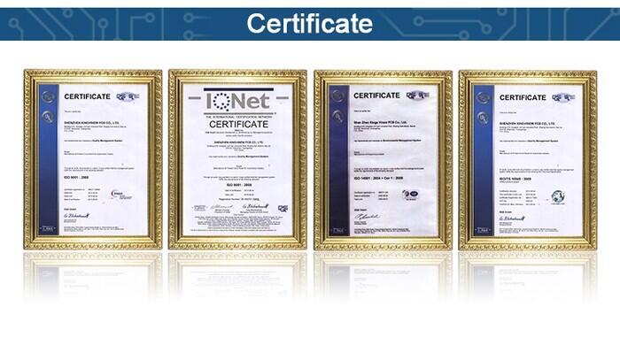
Certificate

