
Search This Supplers Products:BMS Boardaluminium pcbflex PCB boardsmultilayer PCBPCB AssemblyPCB Reverse Engineering
6layer LCD PCB circuit Board For Red Soldermask with Half V-CUT


- group name
- Multilayer PCB Manufacturing
- Min Order
- 1 piece
- brand name
- PCBQuick PCB Manufacturing and Assembly
- model
- KF-Special board
- Nearest port for product export
- SZ
- Delivery clauses under the trade mode
- FOB, EXW, DDU, Express Delivery
- Acceptable payment methods
- T/T, PayPal, Westem Union, Cash, Escrow
- Export mode
- Export through agents
- update time
- Fri, 30 Jul 2021 11:20:07 GMT
Paramtents
Material FR4
Board Thickness 1.6mm
Soldermask Color Red
Silkscreen Color White
Surface Technics ENIG
Min Holes 0.2mm
Min Line space and width 5/5mil
Packging & Delivery
-
Min Order1 piece
Briefing
Routing and V-CUT
Special technics for Half V-CUT, Only V-CUT TOP Layer
Detailed
6layer LCD PCB Board For Red Soldermask with Half V-CUT
Product Description
Material: FR4
Board Thickness: 1.6mm
Copper Thickness: 35um
Soldermask Color: Red
Silkscreen Color: White
Surface Technics: ENIG
Min Holes:0.2mm
Min Line Width and space:5mil/5mil
Special technics for Half V-CUT, Only V-CUT TOP Layer
FR4 Made Ability
| NO | Item | Craft Ability |
|---|---|---|
| 1 | Surface Finishh | HASL,Immersion Gold,Gold Plating,OSP,Immersion Tin,etc |
| 2 | Layer | 2-30 layers |
| 3 | Min. Line Width | 3 mil |
| 4 | Min. Line Space | 3 mil |
| 5 | Min. Space between Pad to Pad | 3 mil |
| 6 | Min.Hole Diameter | 0.10 mm |
| 7 | Min. Bonding Pad Diameter | 10 mil |
| 8 | Max. Proportion of Drilling Hole and Board Thickness | 1:12:5 |
| 9 | Max. Size of Finish Board | 23 inch*35 inch |
| 10 | Rang of Finish Board's Thickness | 0.21-7.0 mm |
| 11 | Min. Thickness of Soldermask | 10 um |
| 12 | Soldermask | Green,Yellow,Black,White,Red,Transparent photosensitive solder mask,Strippable solder mask |
| 13 | Min. Linewidth of Idents | 4 mil |
| 14 | Min. Height of Idents | 25 mil |
| 15 | Color of Silk-screen | White,Yellow,Black |
| 16 | Date File Format | Gerber file and Drilling file,Report series,PADS 2000 series,Powerpcb series,ODB++ |
| 17 | E-testing | 100% E-Testing:High Voltage Testing |
| 18 | Material for PCB | High TG Material:High Frequence (ROGERS,TEFLON,TADONIC,ARLON):Halogen-free Material |
| 19 | Other Test | Impedance Testing,Resistance Testing,Microsection etc |
| 20 | Special Technological Requirement | Blind&Buried Vias and High Thickness Copper |
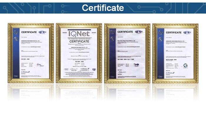
PCB Certificates
UL, TS16949, ISO14001, ISO9001-2008, and RoHS
What is Beneficial to You?
1.You can get high-quality PCB products.
2.You can get a lower price of PCB products to occupy the market.
3.Our one-stop service releases your energy to focus on design and marketing.
4.You can get a strategic long-term partner.
Q:What is the MOQ of the PCB manufacturing?
A:The MOQ is usually 5pcs.
Q: What the package of the PCB products?
A:We use vacuum packaging.
Q:What is the color of the soldermask of the single layer PCB?
A:The solder mask of single layer PCB is green.
Q:What is the color of the silkscreen of the single layer pcb?
A: The color of silkscreen is white.