Search This Supplers Products:BMS Boardaluminium pcbflex PCB boardsmultilayer PCBPCB AssemblyPCB Reverse Engineering
High Frequency PCB Board︱Microwave PCB Fabrication


- group name
- Multilayer PCB Manufacturing
- Min Order
- 1 piece
- brand name
- PCBQuick PCB Manufacturing and Assembly
- model
- KF-High frequency pcb2
- Nearest port for product export
- SZ
- Delivery clauses under the trade mode
- FOB, EXW, DDU, Express Delivery
- Acceptable payment methods
- T/T, PayPal, Westem Union, Cash, Escrow
- Export mode
- Export through agents
- update time
- Fri, 30 Jul 2021 13:52:44 GMT
Paramtents
Soldermask Color Green
Silkscreen Color White
Packging & Delivery
-
Min Order1 piece
Briefing
PCB Sheets:
programmed digital automatic control
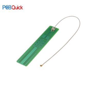
Enhanced wireless network signal
programmed digital automatic control
Enhanced wireless network signal
Detailed
Common type:
1.Double Sided PCB ,Multilayer PCB
Mixed structure: including high performance special plate, P sheet + common performance plate and P sheet mixed pressure structure plate
2.The high frequency substrate + normal FR4 substrate hybrid composite board
3.High frequency substrates + metal based high frequency metal based printing plates
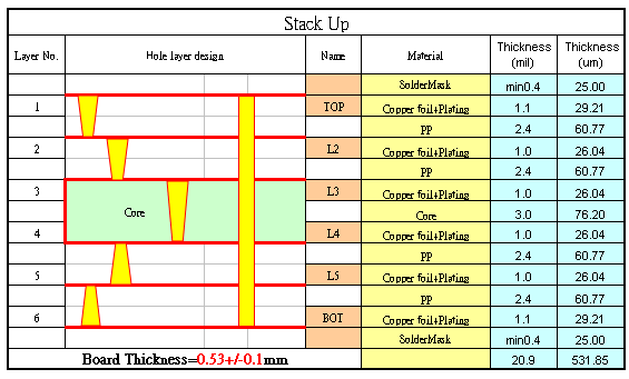
OEM high frequency pcb board stack up

For the characteristics of high speed and high frequency of PCB, two technical approaches are mainly adopted:
1. Make this development into high-density wiring with fine wires and spacing, small aperture, thin shape and conduction, and high reliability of insulation. This can further shorten the signal transmission distance to reduce its loss in transmission.
2. Adopt substrate material with high speed and high frequency characteristics. This requires a deeper understanding of this kind of substrate material, and the research work to find out and master the process method of preparation control, so as to achieve the manufacturing process, performance and cost requirements of the selected substrate material and achieve the goal of reasonable matching.
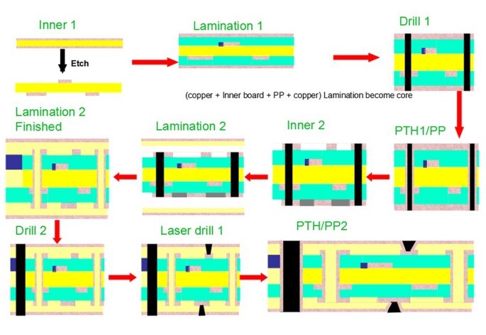
OEM high frequency pcb board Process
Selection of high-frequency materials in design:
1. PCB under 1GHz can be FR4 with low cost and mature multi-layer pressing plate technology.
2. For optical fiber communication products above 622Mb/s and below 3GHz of 1G or above, modified epoxy resin material can be selected. Since the dielectric constant is relatively stable, the cost is lower, and the process of multilayer pressing plate is the same as that of FR4, so as to make multi-layer board, and the cost of the plate is slightly higher than that of FR4.
3.3ghz above signal microwave circuits, such as power amplifiers and low noise amplifiers, are recommended to use plates similar to R04350. The dielectric constant is quite stable, the loss factor is low, the heat resistance is good, and the processing technology is similar to FR4.
Micro blog circuits above 4.10GHz, such as power amplifier, upper and lower frequency converter, have higher requirements for boards. It is recommended to use boards with similar performance to PTFE, or a combination of FR4 and high frequency board glued into low cost, high performance laminate.

OEM high frequency pcb board FAQ
Q : How long does the mass production time of HDI PCB design and manufacture?
A : It is about 10 - 15 working days after confirming of PCB Gerber File.
Q : What color is the solder mask of my design OEM high frequency pcb board?
A : It is black,of course,you can choose another color in your HDI PCB Board.
Q : What kind of surface technics do you use in OEM high frequency pcb board?
A : It usually uses ENIG.
Q : How many layers can you produce of OEM high frequency pcb board ?
A : We can produce multilayer HDI printed circuit board about 4-30 layers.
Q : What is the process capability of OEM high frequency pcb board?
A : Maybe you can see “WHAT PROCESS CAPABILITY CAN WE MAKE FOR HDI PCB” for detailed imformation.
