
Search This Supplers Products:BMS Boardaluminium pcbflex PCB boardsmultilayer PCBPCB AssemblyPCB Reverse Engineering
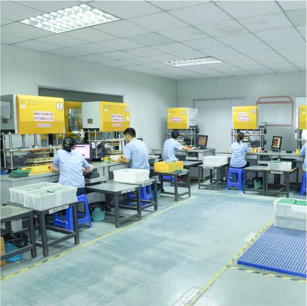
Custom FR4 PCBA PCB Board Assembly Factory in China


- group name
- Telecom PCBA Services
- Min Order
- 1 piece
- brand name
- PCBQuick PCB Manufacturing and Assembly
- model
- KF-FR4 PCB-15
- Nearest port for product export
- SZ
- Delivery clauses under the trade mode
- FOB, EXW, DDU, Express Delivery
- Acceptable payment methods
- T/T, PayPal, Westem Union, Cash, Escrow
- Export mode
- Export through agents
- update time
- Fri, 30 Jul 2021 11:45:03 GMT
Paramtents
Base Material FR4
Copper Thickness 1oz
Board Thickness 1.6mm
Surface Finishing HASL
Min. Hole Size 0.2mm
Min. Line Width 0.1mm
Packging & Delivery
-
Min Order1 piece
Briefing
FR4 PCBA PCB Board Assembly Factory in China
can design all kinds of PCB assembly as you required
can design all kinds of PCB assembly as you required
Detailed
Solder pads and wires on PCB
The element is fixed on the printed circuit board, which is made by welding electrodes to a welded plate. The electrical connection between components depends on printed wires.
1. The welding plate: components through the pin holes on the board, mounted on printed circuit boards with solder welding, printed wire bonding pad have rise, implementation components in the electrical connection in the circuit. The wiring holes and the copper foil around them are welded.
2. Strike and shape of the printed wire: it is naturally preferable that the guide wire shall be printed, which is generally rounded, and the right Angle or included Angle may affect electrical performance in the high frequency circuit.
3. Width of printed conductor: the width of printed conductor can generally be estimated according to 1A/mm. When the power cord and the ground wire are designed, they should be widened appropriately, usually 1.5-2.0mm. If allowed, ground line width > power line width > signal line width. Wide signal lines can be used when the resistance and inductance of the printed circuit board is required. The distance between the lines is usually 1 ~ 1.5mm. Should try to avoid wire cross, if encounter is inevitable, can use jumper length (no more than 25 mm).
Component sub-assembly
1. Needle-type packaging (THT), the component pin will pass through the central hole of the pad through the PCB board at the time of installation, and the properties of the pad Layer are Multi Layer.
2. Tabbed packaging. Pin is attached to the surface of PCB board
PCBA FAQ
Q: What is the MOQ?
A: The minimum order quantity of circuit board is 5pcs.
Q: What the package of the products?
A: We use vacuum packaging.
Q: Do you accept products design with different boards on the same panel?
A: Of course, we can do different boards on the same panel.
Q:What kind of material do you use in my design pcba?
A: We usually use FR4. And you can download FR4 Made Ability.
Q:What color is solder mask usually used in FR4 PCBA?
A : We usually use green in your custom PCBA.
Q: What kind of material do you use on PCBA PCB assembly surface finishing ?
A: FR4 PCB assembly usually uses HASL.